

Himax: Stealth Supplier for NVIDIA's Optics Revolution
$HIMX appears to be manufacturing critical optical components for NVIDIA's AI data center supply chain. Clues indicate it may be supplying Apple's new smart glasses, too.


Authors: Jenny Ahn, Blake Spendley, Sam Koppelman
Editor: Jim Impoco
Based on Hunterbrook Media’s reporting, Hunterbrook Capital is long $HIMX and short a basket of comparable securities at the time of publication. Positions may change at any time. See full disclosures on our website.
Until that moment, it had been a sleepy earnings call.
After detailing the inventory levels of car dashboards and the “seasonal softness” of tablet displays, Himax CEO Jordan Wu sprinkled breadcrumbs that lead straight to the center of the AI revolution.
For over 20 years, Himax Technologies ($HIMX) has been a quiet semiconductor play — a reliable manufacturer of low-margin chips that tell pixels what color to display. To the market, Himax is a relic of the liquid crystal display (LCD) era: the firm that powered the digital photo frame on your grandmother’s mantle and the Face ID on the iPhone X.
But on February 12, Wu signaled a massive opportunity years in the making.
He described an optical product for “the GPU market” that Hunterbrook’s research indicates could one day eclipse his company’s entire $832 million revenue base. He also confirmed a mass-production ramp for a “leading brand’s” smart glasses entering the market this year.
He named neither customer, but the breadcrumbs may be enough.
At Hunterbrook Media — with the help of Citrini Research — we followed a trail of patents, investments, and supply chain shifts. The upshot: The two customers Himax did not name appear to be the two most powerful technology companies in the world. NVIDIA and Apple.
And while investors are still apparently pricing Himax like a commoditized component supplier, the company appears to be emerging as a supplier of a critical optical component powering the next generation of AI data centers.
Getting Light Off the Chip
Last March, Jensen Huang told the world that the networking fabric inside a million-GPU AI factory would consume an amount of electricity rivaling GPUs themselves.
“Energy is our most important commodity,” the NVIDIA CEO said.
Today, fiber optic connections between a network switch and GPU servers rely on a pluggable transceiver, a separate converter box that translates electrical signals to light. A network switch — think of the router in your home, but for AI data centers — routes data between GPU servers.
Each box burns roughly 30 watts. A million-GPU factory requires roughly six transceivers per chip, consuming 180 megawatts of power. To put that in perspective, before a single AI calculation, the networking alone consumes enough electricity to power 150,000 homes.
Huang’s proposed fix: co-packaged optics, or CPO. That’s an optical engine that converts electrons to photons right in the network switch. This eliminates the need for an external transceiver, slashing the power needed for networking by about two-thirds.
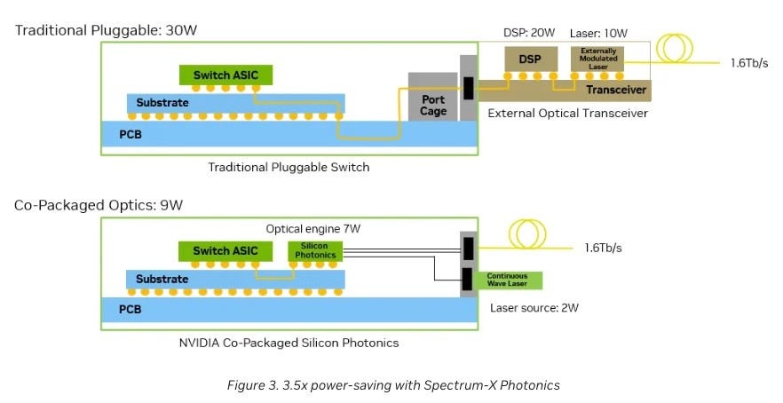
The optical engine is made of silicon chips produced by TSMC ($TSM), the same company that manufactures NVIDIA’s AI chips. The engine doesn’t generate light itself. Instead, it encodes data on a continuous laser beam from an external source. The external laser source modules are built by companies like Lumentum ($LITE) and Coherent ($COHR).
Earlier this month, NVIDIA put its money where its mouth was. The company announced $4 billion in investments split between laser suppliers Lumentum and Coherent, with multibillion-dollar purchase commitments attached. Huang called this investment essential to building “gigawatt-scale AI factories.”
The problem: The optical engine emits its data-carrying light straight up — for one, because it’s easier to test that way.

So something then has to bend each laser 90 degrees — and couple the light into dozens of fibers thinner than a human hair that carry data sideways across the data center.
That something is a prism and a grid of tiny lenses that catch each beam and directs it into the fiber.
Until this point, it has been unclear who would build NVIDIA’s essential light-bending devices.
Our reporting indicates it’s Himax.
How Himax Bends Lasers
Rather than grinding each lens one at a time, Himax stamps batches of them onto a glass wafer in one shot — like pressing a waffle iron into batter — in a process called nanoimprint lithography. Lenses on one side, prisms on the other, all perfectly aligned, according to Himax’s manufacturing patents Hunterbrook reviewed. Himax also uses the same batch process to make the baseplates with grooves shaped like a V that holds each fiber in place.
This isn’t the only way to do it, but “really the best method for doing it,” according to a former Lumentum engineer, referring to the lens-prism scheme. That’s because when you’re dealing with dozens of fibers packed tightly together, mechanically aligning each one becomes a nightmare, he explained to Hunterbrook.
Himax’s array of microlenses and prisms and V-groove baseplates are then integrated into a finished fiber array unit (FAU) by a Taiwanese manufacturer Fiber Optic Communications (TPEX: 3363), according to a FOCI patent Hunterbrook reviewed. FOCI also engineers the intricate connection between the FAU and the optical engine.
This joint Himax-FOCI design and manufacturing process will allow Himax and FOCI to enter the supply chain for TSMC’s COUPE architecture, the optical engine that will power NVIDIA’s CPO platform, according to legendary Apple analyst Ming-Chi Kuo of TF International Securities writing on Medium in December 2024.
Himax and FOCI are finalizing this process “in close collaboration with our anchor customer,” Himax CEO Wu said in a recent earnings call. Wu added Himax is able to manufacture them at mass scale already, and FOCI recently raised $100 million to buy equipment to prepare for mass production.
Shortly after Kuo published his analysis, Digitimes cited TF analysts — without naming them — as confirming Himax as the sole microlens array supplier for COUPE’s first and second generations.1
FOCI and Himax are not entirely independent: In June 2024, Himax invested $16 million for a 5.3% equity stake in FOCI. That stake is now worth around $90 million after a roughly 400% appreciation in FOCI’s share price.
But while FOCI’s valuation has multiplied, Himax’s has largely stagnated — with investors seemingly unaware of its critical role in NVIDIA’s pipeline.
“I think it’s 0% in the stock,” said the physician-turned-investor behind the new Substack Latent Value, which debuted with deep dive research about Himax.
He pointed to Himax’s history of sharp re-ratings once a new product cycle starts. $HIMX hit over $15 during the Google Glass cycle, then surged again on Microsoft HoloLens news.
“It’s at the bottom of the cycle just on the legacy stuff. So that’s what makes it really compelling — even on the legacy business,” he said.
If the Nvidia partnership is confirmed, he says, “the numbers get silly.”
He compared Himax to other companies in NVIDIA’s supply chain like Lumentum and Coherent, similar photonics stocks that have multiplied in value. “Once you’re proven to be in the supply chain for AI, as we’ve seen, stocks can easily 10x and 20x.”
The Patent Trail
The physical evidence goes beyond analyst conjecture.
Four patents — two filed by Himax, one by FOCI, one by TSMC — describe what appears to be the same FAU design and manufacturing process for CPO application. The documents were first unearthed by Latent Value.
A Himax patent published in January details the nanoimprint lithography process for manufacturing the fiber array.2

Then there is TSMC’s December 2025 patent for a FAU inspection tool built specifically for CPO application. The patent describes the schematic of the part being tested — without naming any supplier. But it’s the exact geometric structure that Himax describes: a prism/mirror on one face, microlenses on the other, sitting above a baseplate with fibers. The shape matches. And TSMC’s decision to build a dedicated inspection system for this specific component suggests it’s planning to use it at scale.

And then there is a FOCI patent, filed in late 2024, that adds the finishing touch to what the FAU-COUPE integration might look like.
It describes how to assemble the components of the FAU — the lens array, the prism that bends light, and the V-groove plate — all things that Himax makes. More critically, it describes exactly how the FAU will connect to the COUPE.
The connection is done through the “chip end lens group,” which has a lens part that:
Sits at the bottom of the FAU assembly (chip-facing side)
Can “change the path of the light beam through total reflection” and makes it “reflect and travel upward”
“Can be connected to a chip.”

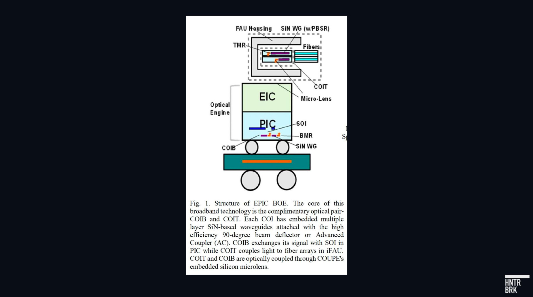
That’s exactly the way TSMC describes its CPO-FAU integration in a recent research paper (also on its website) explaining the optical plumbing on its COUPE platform.
The paper describes a component called COIT — short for Complimentary Optical Interconnect at Top — inside the FAU, equipped with the “high efficiency 90-degree beam deflector” that “couples light to fiber arrays” in the FAU. This is in line with Himax’s design. And, according to TSMC, the COIT is optically coupled with microlenses inside the COUPE.
The paper also says that this method is preferable to the alternative in which the beam is emitted from the side of the optical engine — suggesting TSMC’s decision to choose the light-going-up version was not made in a vacuum, but with a specific FAU in mind to make this version work.
The former Lumentum engineer interviewed by Hunterbrook reviewed the patents — and came away with the conclusion that “there is a high probability that Himax and FOCI are part of the FAU supply chain.”
He cited three main benefits of its technology.
First: “It is a batch process. There are multiple units on a glass wafer that can be processed together.” Second, this process has a lower cost than the traditional lithography process. Third, he added, the optical block using prisms also has higher precision than a mechanical process.
He suspects Himax “is also making some of those microlenses being used in the FAU. That’s why they wrote the wafer level testing patent.”
The patents also reveal intriguing — if speculative — clues to the Himax, FOCI, TSMC supply chain centering on what may be a custom FAU with an unusual specification: a 22-lens array.
In Himax’s January manufacturing patent, a figure illustrating the setup shows the optics block with exactly 22 lenses, if you count the circles representing the lenses.
And a separate patent filed by Himax for testing its prisms says the prism under test “may also be equipped with multiple lenses, such as 16, 22, or 50 lenses, but the number is not limited thereto.”
Twenty-two is an strange number in fiber optics, suggesting it might be custom design. Fiber counts are standardized around specific multiples like 12 or 16; both are numbers you’d see in product specs. Higher-density arrays generally scale in increments of those base units — 24, 32, 48, 72.
But there it is again, in the TSMC’s patent — the closest thing to a smoking gun, though still speculative. TSMC’s inspection schematic explicitly depicts 22 channels, labeled “ch1” through “ch22.”
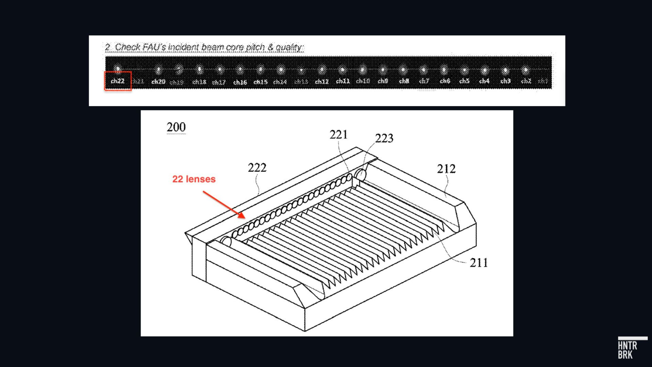
Twenty-two channels appearing in both patents may be a coincidence. But it’s interesting because it appears to describe the same part being inspected at two points in the supply chain: by Himax before shipping, and by TSMC after assembly, before it reaches a GPU.
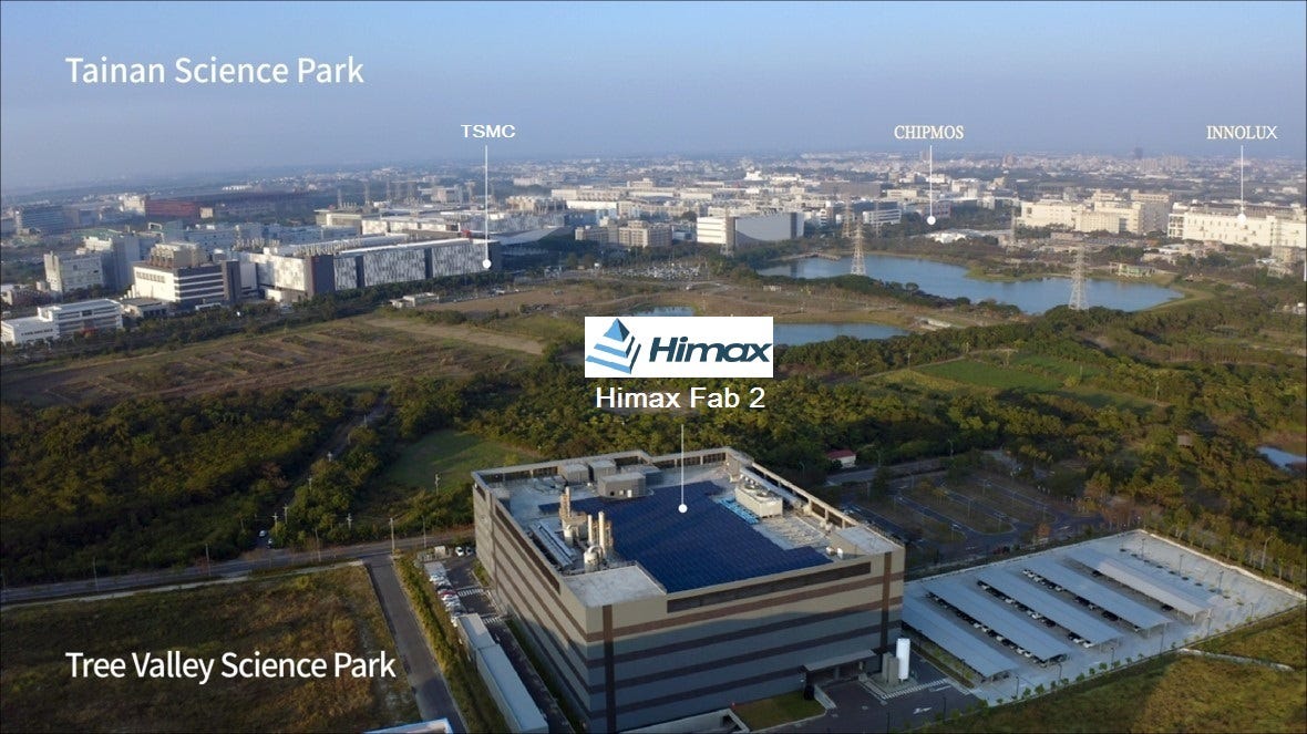
Another plus factor: The company’s short distance from TSMC, as it flexed on a skyline photo of its wafer fab campus posted on its website, suggests the parts wouldn’t be traveling very far. FOCI is just a seven minute drive away as well.
How big is the opportunity?
Morgan Stanley projects 5,000 next-generation NVIDIA Rubin Ultra racks shipping in 2027 and 28,000 in 2028.
Even using conservative pricing assumptions, the FAU market scales from hundreds of millions in 2027 to billions of dollars in 2028, according to Citrini Research’s analysis. And NVIDIA’s Feynman architecture — the generation planned for after Rubin — is expected to multiply the unit count further.
The Apple Opportunity
On the earnings call last month, Wu, the Himax CEO, disclosed that a top smart glasses brand would enter mass production by the end of 2026.
Himax has described three core technologies that could become essential to this space: its WiseEye AI sensing processor, its tiny projection display known as LCoS microdisplay, and its compatibility with waveguide — the optical layers that make see-through displays possible.
Wu has not named the smart glasses brand. He might not have needed to.
DigiTimes reported in early February that Apple’s expected smart glasses entry is reshaping the Taiwanese augmented reality (AR) optics supply chain, with multiple suppliers increasing capex in anticipation. The Apple analyst Ming-Chi Kuo, known for predicting the company’s releases, anticipates mass production beginning soon en route to a 2027 launch, a similar timeline to the one reported by Bloomberg.
Kuo projects Apple’s first smart glasses will ship 3 million to 5 million units in the launch year. These would likely be audio only, not requiring extensive purchases from Himax. And then, the potential transformative opportunity would arrive in 2028, when Kuo says Apple is expected to launch display-equipped AR glasses using LCoS microdisplays and waveguides. That’s where Himax would come in.
Himax’s relationship with Apple would not be new.
In 2017, Himax was reported (see this, this, this, and this) as a key supplier of the wafer-level optics that power Face ID on the iPhone X — the tiny dot-projector lenses that map a user’s face in three dimensions.
In the smart glasses supply chain, Himax may occupy a specific niche.
Karl Guttag is a former Texas Instruments Fellow with 40 years of experience in display technology, who founded an LCoS company and now runs KGOnTech, a popular independent technical blog in the AR/VR industry. He’s tracked Himax since the Google Glass era, when his identification of Himax as its LCoS supplier allegedly moved the company’s market cap by more than $100 million in a single day.
He described Himax to Hunterbrook as “a little bit the McDonald’s of the LCoS world” — not the highest quality, but able to produce massive volume. “They’ve never had the best LCoS,” Guttag said. “They’re kind of the low-cost guy.”
Historically, Himax has partnered with top companies on microdisplays, including the original Microsoft HoloLens and Google Glass and other AR platforms. More recently, at CES 2026, Himax and smart glasses maker Vuzix ($VUZI) unveiled an optical reference design pairing Himax’s ultra-compact Front-lit LCoS microdisplay with Vuzix’s waveguide.
If involved with Apple, Himax would “probably” be supplying “the LCoS and the waveguide,” Guttag conjectured. Himax’s wafer fab facilities — the same ones that fabricate microlens and V-groove baseplates using nanoimprint lithography — have already churned out thousands of waveguide displays in the past, and Wu recently talked on earnings calls about using its facilities for fabricating waveguide optics for other companies’ designs. But Guttag also questioned the fit: “Himax has never demonstrated the highest quality LCoS nor the highest quality waveguides,” he told Hunterbrook.
Guttag noted that Apple may be driven by capacity goals: Himax is “in the best capacity situation” among LCoS makers, he said. He suggested Apple’s choice may reflect pragmatism over perfectionism: “Maybe they’re more controllable, or they had the capacity.”
Although there is no direct confirmation that Himax has once again partnered with Apple, there’s circumstantial evidence — including on LinkedIn.
One profile of interest allegedly belongs to someone describing themselves as a Himax senior product manager with the title “Advanced Optics & NPI Integration | Apple Project Lead.” This individual — whose identity is labeled as “verified” on LinkedIn — claims to have previously led the Meta Quest 3 lens program, scaling production to over 7 million units.
Their recent posts describe shipping ahead of customer deadlines and resolving late-stage manufacturing defects, language consistent with a program approaching production ramp.
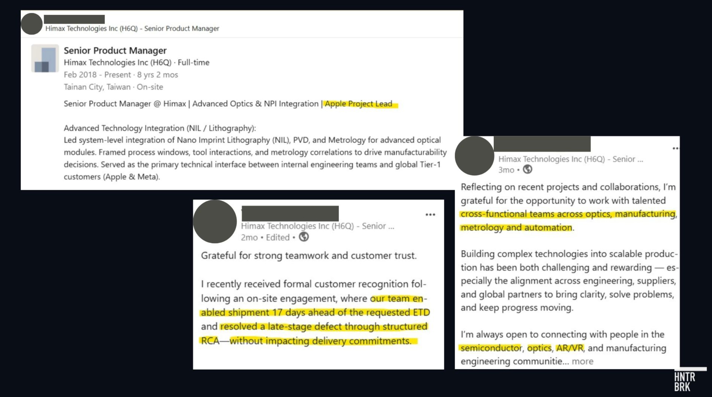
Then, as Hunterbrook prepared to publish this article, they posted again: “Visiting Apple Park this week for technical discussions and collaboration.”

Hunterbrook geolocated the image and tracked the aircraft, EVA’s B-16716, revealing that the senior product manager appears to have flown from Taipei to San Francisco on Monday, March 9.3

Asked whether it could confirm its relationships with Apple and Nvidia, Himax did not respond to Hunterbrook’s request for comment, and TSMC declined to comment. The purported employee on LinkedIn who posted the flight did not respond to direct messages. And Hunterbrook has not been able to match their identity on any other social media platforms — though we did find a master’s thesis on a Taiwanese academic research database from a student of the same name from the same graduate school at the same rough time period this purported Himax employee lists on LinkedIn. LinkedIn also claims the account was “verified” with a government ID.
And on Monday, the employee posted again: “Day 1 at Apple Park — a full day of technical discussions and collaboration, from 11am to 9pm. Productive start to the week.”
One of the images attached to the post? A selfie in front of Norman Foster’s signature Apple Park design, including the internal arbor of the headquarters, known as “the spaceship.” This area is closed to the public.


We geolocated the image. It’s clearly inside of the secure perimeter.
“I’m amazed that somebody would post something like that,” said Guttag.
Authors
Sam Koppelman is a New York Times best-selling author who has written books with former United States Attorney General Eric Holder and former United States Acting Solicitor General Neal Katyal. Sam has published in the New York Times, Washington Post, Boston Globe, Time Magazine, and other outlets. He has a B.A. in Government from Harvard, where he was named a John Harvard Scholar and wrote op-eds like “Shut Down Harvard Football,” which he tells us were great for his social life.
Jenny Ahn joined Hunterbrook after serving many years as a senior analyst in the US government. She is a seasoned geopolitical expert with a particular focus on the Asia-Pacific and has diverse overseas experience. She has an M.A. in International Affairs from Yale and a B.S. in International Relations from Stanford. Jenny is based in Virginia.
Blake Spendley joined Hunterbrook from the Center for Naval Analyses (CNA), where he led investigations as a Research Specialist for the Marine Corps and US Navy. He built and owns the leading open-source intelligence (OSINT) account on X/Twitter, called @OSINTTechnical (over 1 million followers), which also distributes Hunterbrook Media reporting. His OSINT research has been published in Bloomberg, the Wall Street Journal, and The Economist, among other top business outlets. He has a B.A. in Political Science from USC.
Editor
Jim Impoco is the award-winning former editor-in-chief of Newsweek who returned the publication to print in 2014. Before that, he was executive editor at Thomson Reuters Digital, Sunday Business Editor at The New York Times, and Assistant Managing Editor at Fortune. Jim, who started his journalism career as a Tokyo-based reporter for The Associated Press and U.S. News & World Report, has a master’s in Chinese and Japanese History from the University of California at Berkeley.
Graphic
Dan DeLorenzo is a creative director with 25 years reporting news through visuals. Since first joining a newsroom graphics department in 2001, he has built teams at Bloomberg News, Bridgewater Associates, and the United Nations, and published groundbreaking visual journalism at The Wall Street Journal, Associated Press, The New York Times, and Business Insider. A passion for the craft has landed him at the helm of newsroom teams, on the ground in humanitarian emergencies, and at the epicenter of the world’s largest hedge fund. He runs DGFX Studio, a creative agency serving top organizations in media, finance, and civil society with data visualization, cartography, and strategic visual intelligence. He moonlights as a professional sailor working toward a USCG captain’s license and is a certified Pilates instructor.
Hunterbrook Media publishes investigative and global reporting — with no ads or paywalls. When articles do not include Material Non-Public Information (MNPI), or “insider info,” they may be provided to our affiliate Hunterbrook Capital, an investment firm which may take financial positions based on our reporting. Subscribe here. Learn more here.
Please contact ideas@hntrbrk.com to share ideas, talent@hntrbrk.com for work opportunities, and press@hntrbrk.com for media inquiries.
LEGAL DISCLAIMER
© 2026 by Hunterbrook Media LLC. When using this website, you acknowledge and accept that such usage is solely at your own discretion and risk. Hunterbrook Media LLC, along with any associated entities, shall not be held responsible for any direct or indirect damages resulting from the use of information provided in any Hunterbrook publications. It is crucial for you to conduct your own research and seek advice from qualified financial, legal, and tax professionals before making any investment decisions based on information obtained from Hunterbrook Media LLC. The content provided by Hunterbrook Media LLC does not constitute an offer to sell, nor a solicitation of an offer to purchase any securities. Furthermore, no securities shall be offered or sold in any jurisdiction where such activities would be contrary to the local securities laws.
Hunterbrook Media LLC is not a registered investment advisor in the United States or any other jurisdiction. We strive to ensure the accuracy and reliability of the information provided, drawing on sources believed to be trustworthy. Nevertheless, this information is provided “as is” without any guarantee of accuracy, timeliness, completeness, or usefulness for any particular purpose. Hunterbrook Media LLC does not guarantee the results obtained from the use of this information. All information presented are opinions based on our analyses and are subject to change without notice, and there is no commitment from Hunterbrook Media LLC to revise or update any information or opinions contained in any report or publication contained on this website. The above content, including all information and opinions presented, is intended solely for educational and information purposes only. Hunterbrook Media LLC authorizes the redistribution of these materials, in whole or in part, provided that such redistribution is for non-commercial, informational purposes only. Redistribution must include this notice and must not alter the materials. Any commercial use, alteration, or other forms of misuse of these materials are strictly prohibited without the express written approval of Hunterbrook Media LLC. Unauthorized use, alteration, or misuse of these materials may result in legal action to enforce our rights, including but not limited to seeking injunctive relief, damages, and any other remedies available under the law.
The partnership between the two companies was publicly tested in January — when Taiwan’s Economic Daily News reported that Largan Precision (TPE: 3008) — Taiwan’s dominant smartphone lens manufacturer, with a market cap exceeding $9 billion — had partnered with TSMC to supply optical elements for CPO, and had already sent samples for testing on what the paper described as an AMD project. The report claimed Largan was leveraging its precision optics alignment technology to position itself as an alternative to Himax, and that Largan had established an emergency CPO production line at its new factory. Himax responded that same evening with a formal press release confirming that “all ongoing collaborations between the two parties continue to progress actively, and there has been no change.” In a note, Morgan Stanley said: “Our checks suggest Himax remains FOCI’s sole FAU supplier for both scale-out and scale-out CPO solutions. We do not rule out a second source in the long run given significant CPO demand, but mass-production experience and yield rate are still the priorities.”
This is a divisional patent that divides into two separate patents: one protecting the physical design of the fiber array (claims 1–6), and one protecting the nanoimprint lithography manufacturing method (claims 7–15). It’s standard but deliberate patent strategy. The timing suggests Himax’s patent counsel is actively fortifying the IP moat around the nanoimprint lithography process specifically./hb_annotation] It describes stamping patterns onto glass wafers using molds to create a “plurality” of optical components on a single wafer: an optics block with lenses imprinted on one face of a glass wafer and 45-degree prisms on the other, as well as a V-groove plate for holding the fibers in place. It’s a “low-cost, high throughput and high resolution” process “suitable for mass production,” the patent claims.
Using the aircraft’s tail number, we pulled its flight history on Flightradar24. We also matched key visual elements, like the tarmac markings, to gate C9 in Taipei.